Capacitance Meter Circuit

OVERVIEW

My linear and digital circuits class ended in a term-long design project: build a breadboard circuit that takes an unknown capacitor and reports its value as a voltage you can read. I had been looking for a reason to spend real time at a bench with an oscilloscope, and this turned into a term of exactly that!

YEAR

2026

ROLE

Circuit Design Co-Lead

SKILLS GAINED

Analog & Digital Circuit Design
Oscilloscope Debugging
Simulation vs. Reality

About the project

Context

ENGS 32 culminates in a design project, and my partner Nate and I were handed a spec rather than a schematic: measure a test capacitor across at least two decades of value, run the analog section off a +9/-9 V supply, and output a voltage that maps to capacitance. Everything else was ours to figure out.

The starting point is the current-voltage relationship of a capacitor, i(t) = C dv/dt. If you drive a capacitor with a steady AC signal, the current through it scales with its capacitance, so measuring that current tells you the value. A capacitor blocks DC, which is why an oscillator is the first block in the chain and not a bench supply. Converting that small current into a readable voltage is what a transimpedance amplifier does, so the core of the design came together quickly.

The hard part was range. A single fixed gain either clips the supply rails on a large capacitor or buries a small one in the noise floor, so covering multiple decades meant the circuit had to decide which decade it was in and change its own gain to match. That requirement is what pulled a whole digital half into what started as an analog project.

Process

Our first design idea was two separate gain op-amps, one at 5x and one at 50x, with a multiplexer switched by comparators to pick between them. In our first design review, our professor and lab instructor wisely took that apart and pointed us at something much simpler: one gain stage that sits at 1x, with an NPN transistor that switches in a second feedback resistor to make it 10x when the logic tells it to. Same result, a fraction of the parts.

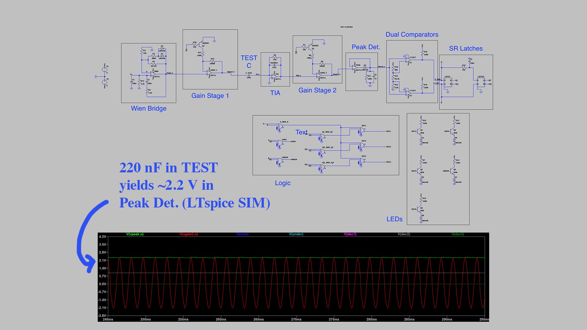
From there the chain settled into: a Wien bridge oscillator generates a steady sine wave, a first gain stage boosts it, the test capacitor passes current, the TIA converts that current to a voltage, a second gain stage scales it, a peak detector holds the AC maximum as a DC level, and two comparators feed SR latches that decide which decade we are in and switch the gain transistors. Five LEDs report the state: Under, Decade 1, Decade 2, Decade 3, Over.

One decision I still like is putting the two gain stages on opposite sides of the test capacitor. The first one makes sure enough current flows through the capacitor to be detected at all, and the second makes sure the voltage coming out of the TIA is large enough to be processed reliably. Amplifying as close to the source as possible keeps noise down, so the stage before the capacitor does the work for the middle range.

We proved the concept in LTspice first, then built on the breadboard one block at a time, checking each stage on the oscilloscope against the time-domain equation before adding the next. With 22 nF in the socket the Wien bridge measured 652 Hz at 500 mV, gain stage 1 brought it to about 5 V, and the TIA came out as an inverted cosine shifted 93 degrees from its input, which is what the math predicted. Once two decades worked, we added a third (0.5 to 5 µF), which meant a second gain stage plus another SR latch, NOR gate, and inverter to hold the extra state.

Dose Calculations
Numerous Deposition Failures

Challenges

The build was the biggest time sink of the project, and most of it was self-inflicted. We jumped straight into building the analog and digital halves at once instead of finishing one and then starting the other, and the board got crowded enough that we reordered components several times and eventually swapped breadboards entirely over a fault we could not find. We did draw a full board layout on paper, but we should have drawn it before building rather than partway through.

LTspice was useful and also a little misleading. A simulation has no parasitic resistance, no stray capacitance, and no noise, so the first physical version of each stage rarely behaved like the simulated one. We added a potentiometer to the Wien bridge so we could set the input amplitude precisely instead of trusting resistor values, and the multimeter got as much use as the scope, checking op-amp pins one at a time to find where a signal died. At one point we ran out of NPN transistors for the LED drivers, and our lab instructor Bob got us around it by running the LEDs off the supply rails instead.

My favorite failure showed up in the third decade. As capacitance increased, the output voltage tapered off instead of scaling linearly, and we did not solve it until after the live demo. The cause was the 47 Ω stabilizer resistor at the TIA input: at large test capacitances it started dominating the input impedance and formed a low-pass filter we never intended to build, rolling off exactly the signals we were trying to measure. Removing it restored linearity in the third decade without touching the first two. It was a good lesson in how a component you added for stability can quietly become the thing limiting your measurement.

Aluminum Evaporation Deposition
Gold Sputtering Trial

Conclusion

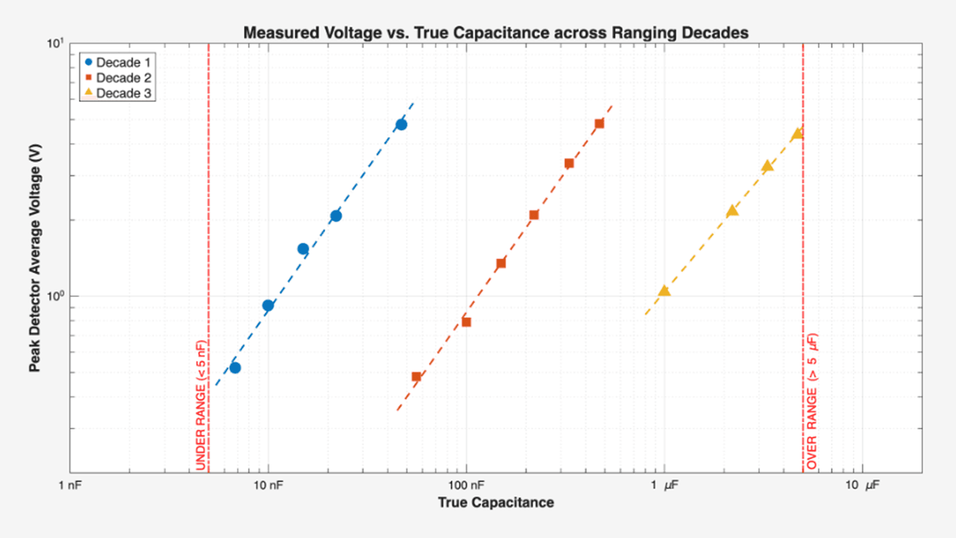
Sweeping capacitors from 4.7 nF to 10 µF, the meter identified the correct decade every time, flagged the two out-of-range parts as Under and Over, and tracked capacitance with an average accuracy of 92.46%. Plotting output voltage against true capacitance gave slopes of 1.04, 1.07, and 0.90 across the three decades, so each range was close to the linear response we designed for.

The errors were not spread evenly, and where they landed is the more interesting result. Our best readings came in near 1.5% while the worst sat at the bottom edge of each decade, where the output voltage is smallest and the signal is closest to the noise. That points at a few causes: capacitive impedance goes as 1/(2πfC), so at the low end of a range the current through the capacitor is small and the signal-to-noise ratio suffers, and our components were only rated to ±5% themselves, so part of what we measured was the capacitors and not the meter.

This project was the first time I designed something from a specification rather than a lab handout, and the part that stuck with me is how much of it happened on the bench rather than on paper. The equations told us what each stage should do, and the oscilloscope told us what it actually did, and closing the gap between those two was the real work. Thank you to Professor Farnham and our technical instructor Bob Barry for the design reviews that saved us from ourselves, and to my friend Nate for being a great partner!

The Cleanroom We Utilized
One Successfully Manufactured Resistor
Smooth Scroll
This will hide itself!

Capacitance Meter Circuit

OVERVIEW

My linear and digital circuits class ended in a term-long design project: build a breadboard circuit that takes an unknown capacitor and reports its value as a voltage you can read. I had been looking for a reason to spend real time at a bench with an oscilloscope, and this turned into a term of exactly that!

YEAR

2026

ROLE

Circuit Design Co-Lead

SKILLS GAINED

Analog & Digital Circuit Design
Oscilloscope Debugging
Simulation vs. Reality

About the project

Context

ENGS 32 culminates in a design project, and my partner Nate and I were handed a spec rather than a schematic: measure a test capacitor across at least two decades of value, run the analog section off a +9/-9 V supply, and output a voltage that maps to capacitance. Everything else was ours to figure out.

The starting point is the current-voltage relationship of a capacitor, i(t) = C dv/dt. If you drive a capacitor with a steady AC signal, the current through it scales with its capacitance, so measuring that current tells you the value. A capacitor blocks DC, which is why an oscillator is the first block in the chain and not a bench supply. Converting that small current into a readable voltage is what a transimpedance amplifier does, so the core of the design came together quickly.

The hard part was range. A single fixed gain either clips the supply rails on a large capacitor or buries a small one in the noise floor, so covering multiple decades meant the circuit had to decide which decade it was in and change its own gain to match. That requirement is what pulled a whole digital half into what started as an analog project.

Process

Our first design idea was two separate gain op-amps, one at 5x and one at 50x, with a multiplexer switched by comparators to pick between them. In our first design review, our professor and lab instructor wisely took that apart and pointed us at something much simpler: one gain stage that sits at 1x, with an NPN transistor that switches in a second feedback resistor to make it 10x when the logic tells it to. Same result, a fraction of the parts.

From there the chain settled into: a Wien bridge oscillator generates a steady sine wave, a first gain stage boosts it, the test capacitor passes current, the TIA converts that current to a voltage, a second gain stage scales it, a peak detector holds the AC maximum as a DC level, and two comparators feed SR latches that decide which decade we are in and switch the gain transistors. Five LEDs report the state: Under, Decade 1, Decade 2, Decade 3, Over.

One decision I still like is putting the two gain stages on opposite sides of the test capacitor. The first one makes sure enough current flows through the capacitor to be detected at all, and the second makes sure the voltage coming out of the TIA is large enough to be processed reliably. Amplifying as close to the source as possible keeps noise down, so the stage before the capacitor does the work for the middle range.

We proved the concept in LTspice first, then built on the breadboard one block at a time, checking each stage on the oscilloscope against the time-domain equation before adding the next. With 22 nF in the socket the Wien bridge measured 652 Hz at 500 mV, gain stage 1 brought it to about 5 V, and the TIA came out as an inverted cosine shifted 93 degrees from its input, which is what the math predicted. Once two decades worked, we added a third (0.5 to 5 µF), which meant a second gain stage plus another SR latch, NOR gate, and inverter to hold the extra state.
Dose Calculations
Numerous Deposition Failures

Challenges

The build was the biggest time sink of the project, and most of it was self-inflicted. We jumped straight into building the analog and digital halves at once instead of finishing one and then starting the other, and the board got crowded enough that we reordered components several times and eventually swapped breadboards entirely over a fault we could not find. We did draw a full board layout on paper, but we should have drawn it before building rather than partway through.

LTspice was useful and also a little misleading. A simulation has no parasitic resistance, no stray capacitance, and no noise, so the first physical version of each stage rarely behaved like the simulated one. We added a potentiometer to the Wien bridge so we could set the input amplitude precisely instead of trusting resistor values, and the multimeter got as much use as the scope, checking op-amp pins one at a time to find where a signal died. At one point we ran out of NPN transistors for the LED drivers, and our lab instructor Bob got us around it by running the LEDs off the supply rails instead.

My favorite failure showed up in the third decade. As capacitance increased, the output voltage tapered off instead of scaling linearly, and we did not solve it until after the live demo. The cause was the 47 Ω stabilizer resistor at the TIA input: at large test capacitances it started dominating the input impedance and formed a low-pass filter we never intended to build, rolling off exactly the signals we were trying to measure. Removing it restored linearity in the third decade without touching the first two. It was a good lesson in how a component you added for stability can quietly become the thing limiting your measurement.

Aluminum Evaporation Deposition
Gold Sputtering Trial

Conclusion

Sweeping capacitors from 4.7 nF to 10 µF, the meter identified the correct decade every time, flagged the two out-of-range parts as Under and Over, and tracked capacitance with an average accuracy of 92.46%. Plotting output voltage against true capacitance gave slopes of 1.04, 1.07, and 0.90 across the three decades, so each range was close to the linear response we designed for.

The errors were not spread evenly, and where they landed is the more interesting result. Our best readings came in near 1.5% while the worst sat at the bottom edge of each decade, where the output voltage is smallest and the signal is closest to the noise. That points at a few causes: capacitive impedance goes as 1/(2πfC), so at the low end of a range the current through the capacitor is small and the signal-to-noise ratio suffers, and our components were only rated to ±5% themselves, so part of what we measured was the capacitors and not the meter.

This project was the first time I designed something from a specification rather than a lab handout, and the part that stuck with me is how much of it happened on the bench rather than on paper. The equations told us what each stage should do, and the oscilloscope told us what it actually did, and closing the gap between those two was the real work. Thank you to Professor Farnham and our technical instructor Bob Barry for the design reviews that saved us from ourselves, and to my friend Nate for being a great partner!

The Cleanroom We Utilized
One Successfully Manufactured Resistor
Smooth Scroll
This will hide itself!

Capacitance Meter Circuit

OVERVIEW

My linear and digital circuits class ended in a term-long design project: build a breadboard circuit that takes an unknown capacitor and reports its value as a voltage you can read. I had been looking for a reason to spend real time at a bench with an oscilloscope, and this turned into a term of exactly that!

YEAR

2026

ROLE

Circuit Design Co-Lead

SKILLS GAINED

Analog & Digital Circuit Design
Oscilloscope Debugging
Simulation vs. Reality

About the project

Context

ENGS 32 culminates in a design project, and my partner Nate and I were handed a spec rather than a schematic: measure a test capacitor across at least two decades of value, run the analog section off a +9/-9 V supply, and output a voltage that maps to capacitance. Everything else was ours to figure out.

The starting point is the current-voltage relationship of a capacitor, i(t) = C dv/dt. If you drive a capacitor with a steady AC signal, the current through it scales with its capacitance, so measuring that current tells you the value. A capacitor blocks DC, which is why an oscillator is the first block in the chain and not a bench supply. Converting that small current into a readable voltage is what a transimpedance amplifier does, so the core of the design came together quickly.

The hard part was range. A single fixed gain either clips the supply rails on a large capacitor or buries a small one in the noise floor, so covering multiple decades meant the circuit had to decide which decade it was in and change its own gain to match. That requirement is what pulled a whole digital half into what started as an analog project.

Process

Our first design idea was two separate gain op-amps, one at 5x and one at 50x, with a multiplexer switched by comparators to pick between them. In our first design review, our professor and lab instructor wisely took that apart and pointed us at something much simpler: one gain stage that sits at 1x, with an NPN transistor that switches in a second feedback resistor to make it 10x when the logic tells it to. Same result, a fraction of the parts.

From there the chain settled into: a Wien bridge oscillator generates a steady sine wave, a first gain stage boosts it, the test capacitor passes current, the TIA converts that current to a voltage, a second gain stage scales it, a peak detector holds the AC maximum as a DC level, and two comparators feed SR latches that decide which decade we are in and switch the gain transistors. Five LEDs report the state: Under, Decade 1, Decade 2, Decade 3, Over.

One decision I still like is putting the two gain stages on opposite sides of the test capacitor. The first one makes sure enough current flows through the capacitor to be detected at all, and the second makes sure the voltage coming out of the TIA is large enough to be processed reliably. Amplifying as close to the source as possible keeps noise down, so the stage before the capacitor does the work for the middle range.

We proved the concept in LTspice first, then built on the breadboard one block at a time, checking each stage on the oscilloscope against the time-domain equation before adding the next. With 22 nF in the socket the Wien bridge measured 652 Hz at 500 mV, gain stage 1 brought it to about 5 V, and the TIA came out as an inverted cosine shifted 93 degrees from its input, which is what the math predicted. Once two decades worked, we added a third (0.5 to 5 µF), which meant a second gain stage plus another SR latch, NOR gate, and inverter to hold the extra state.

Dose Calculations
Numerous Deposition Failures

Challenges

The build was the biggest time sink of the project, and most of it was self-inflicted. We jumped straight into building the analog and digital halves at once instead of finishing one and then starting the other, and the board got crowded enough that we reordered components several times and eventually swapped breadboards entirely over a fault we could not find. We did draw a full board layout on paper, but we should have drawn it before building rather than partway through.

LTspice was useful and also a little misleading. A simulation has no parasitic resistance, no stray capacitance, and no noise, so the first physical version of each stage rarely behaved like the simulated one. We added a potentiometer to the Wien bridge so we could set the input amplitude precisely instead of trusting resistor values, and the multimeter got as much use as the scope, checking op-amp pins one at a time to find where a signal died. At one point we ran out of NPN transistors for the LED drivers, and our lab instructor Bob got us around it by running the LEDs off the supply rails instead.

My favorite failure showed up in the third decade. As capacitance increased, the output voltage tapered off instead of scaling linearly, and we did not solve it until after the live demo. The cause was the 47 Ω stabilizer resistor at the TIA input: at large test capacitances it started dominating the input impedance and formed a low-pass filter we never intended to build, rolling off exactly the signals we were trying to measure. Removing it restored linearity in the third decade without touching the first two. It was a good lesson in how a component you added for stability can quietly become the thing limiting your measurement.

Aluminum Evaporation Deposition
Gold Sputtering Trial

Conclusion

Sweeping capacitors from 4.7 nF to 10 µF, the meter identified the correct decade every time, flagged the two out-of-range parts as Under and Over, and tracked capacitance with an average accuracy of 92.46%. Plotting output voltage against true capacitance gave slopes of 1.04, 1.07, and 0.90 across the three decades, so each range was close to the linear response we designed for.

The errors were not spread evenly, and where they landed is the more interesting result. Our best readings came in near 1.5% while the worst sat at the bottom edge of each decade, where the output voltage is smallest and the signal is closest to the noise. That points at a few causes: capacitive impedance goes as 1/(2πfC), so at the low end of a range the current through the capacitor is small and the signal-to-noise ratio suffers, and our components were only rated to ±5% themselves, so part of what we measured was the capacitors and not the meter.

This project was the first time I designed something from a specification rather than a lab handout, and the part that stuck with me is how much of it happened on the bench rather than on paper. The equations told us what each stage should do, and the oscilloscope told us what it actually did, and closing the gap between those two was the real work. Thank you to Professor Farnham and our technical instructor Bob Barry for the design reviews that saved us from ourselves, and to my friend Nate for being a great partner!

The Cleanroom We Utilized
One Successfully Manufactured Resistor
Smooth Scroll
This will hide itself!